PCB Design - 45 Days Internship Training Program
Join 45 Days PCB Design Internship Training Program at NextVision Infotech. Learn schematic, layout, routing, Gerber, manufacturing. ₹649 only with certificate.
Program Description
Skills You'll Learn
Projects You'll Work On
Complete PCB Design Project
Students will complete a full PCB design project including schematic capture, footprint creation, layout design, routing, DRC, Gerber generation, drill files, BOM, assembly documentation, and complete project documentation as per industry standards.
Program Modules
W1: Week 1: PCB Fundamentals and Design Flow
Introduction to PCB, history of PCB, types of PCB - single layer, double layer, multi-layer, rigid, flexible, rigid-flex, PCB materials - FR4, CEM-1, CEM-3, metal core, PCB components - through-hole, SMD, BGA, QFN, QFP, PCB design flow, schematic capture, netlist generation, footprint assignment, layout design, routing, design rule check, Gerber generation, PCB manufacturing, assembly, PCB standards, IPC standards, PCB design software - KiCad, EasyEDA, Altium Designer, Eagle, OrCAD, Proteus.
W2: Week 2: Schematic Capture
Schematic design fundamentals, schematic symbols, component selection, resistor, capacitor, inductor, diode, transistor, MOSFET, IC, connector, crystal, schematic editor, placing components, wiring, net labels, bus, hierarchical design, sheet symbols, global labels, power ports, ERC (Electrical Rule Check), netlist generation, BOM generation, schematic documentation, schematic best practices, schematic review.
W3: Week 3: Footprint Creation and Component Libraries
Footprint fundamentals, through-hole footprints, SMD footprints, pad shapes, pad sizes, pad spacing, courtyard, silkscreen, assembly layer, 3D models, IPC footprint standards, IPC-7351, footprint creation, footprint editor, library management, component libraries, symbol libraries, footprint libraries, 3D model libraries, library creation, library verification, library best practices.
W4: Week 4: Layout Design and Routing
PCB layout fundamentals, board outline, board size, layer stackup, layer selection, component placement, placement guidelines, thermal considerations, signal integrity, power integrity, EMI/EMC considerations, routing, trace width calculation, trace spacing, differential pairs, length matching, impedance control, vias, via types, blind vias, buried vias, microvias, copper pour, ground plane, power plane, thermal relief, design rule check (DRC), layout optimization.
W5: Week 5: Advanced Design Techniques, Manufacturing, and Live Projects
Advanced PCB design techniques, high-speed design, RF design, mixed-signal design, analog-digital separation, grounding techniques, shielding, decoupling capacitors, power distribution network, PCB manufacturing process, PCB fabrication, photolithography, etching, drilling, plating, solder mask, silkscreen, surface finish - HASL, ENIG, OSP, immersion silver, immersion tin, PCB assembly, SMT assembly, through-hole assembly, reflow soldering, wave soldering, Gerber generation, drill files, pick and place files, live projects - Arduino board, power supply board, microcontroller board, sensor board, complete documentation.
W6: Week 6: Documentation, Viva, and Certification
Project documentation, schematic documentation, layout documentation, Gerber documentation, BOM documentation, assembly documentation, design review, DFM (Design for Manufacturing), DFA (Design for Assembly), DFT (Design for Test), project report preparation, resume building, interview preparation, viva-voce examination, feedback session, certificate distribution.
Key Features
What You'll Learn
Examination Details
| Exam Name | Full Marks | Pass Marks |
|---|---|---|
| Module-wise Assessment | 100 | 40 |
| Project Evaluation | 100 | 50 |
| Final Presentation | 50 | 25 |
| Viva-Voce | 50 | 25 |
Internship Details
Prerequisites
- Pursuing or completed B.Tech/B.E./Diploma in Electronics, ECE, EEE, or related field
- Basic knowledge of electronics circuits
- Basic knowledge of electronic components
- Interest in PCB design
Who Can Enroll ?
- B.Tech ECE students (1st to 8th semester)
- B.E. ECE students
- B.Tech Electronics Engineering students
- B.Tech Electrical Engineering students
- Diploma Electronics students (1st to 6th semester)
- Polytechnic students
- Working professionals wanting to upskill
- Students from all over India seeking practical training
Certificate Preview

Related Internships
You might also be interested in these
Embedded Systems - 45 Days Internship Training Program
Join 45 Days Embedded Systems Internship Training Progr...
Internet of Things (IoT) - 45 Days Internship Training Program
Join 45 Days Internet of Things (IoT) Internship Traini...
Innovative Hardware Design for Biomedical Robotics - 1 Month Internship Training Program
Join 1 Month Innovative Hardware Design for Biomedical...
Our Students Did It!
Real stories, real success. See how NextVision Infotech helped our students build their careers.

Karan Bahadur Thapa
Internship Program
"Best decision I ever made! The teaching quality and practical training helped me land my dream job. Highly recommended! 🌟"

Diptangshu De
Internship Program
"Amazing experience! The mentors are super supportive and the course content is industry-ready. Got my certificate with confidence! 💯"

Ansh Verma
Internship Program
"NVI Gaya changed my career path completely. Practical projects, real-world skills, and expert guidance — everything was perfect! 🚀"
Rishu kumari
Internship Program
"Learned so much in such a short time. The internship gave me real experience and confidence to face interviews. Thank you NVI! 🙏"

Rishabh malviya
Internship Program
"Best decision I ever made! The teaching quality and practical training helped me land my dream job. Highly recommended! 🌟"

Kishan Shukla
Internship Program
"Amazing experience! The mentors are super supportive and the course content is industry-ready. Got my certificate with confidence! 💯"

Saquib kausar
Internship Program
"NVI Gaya changed my career path completely. Practical projects, real-world skills, and expert guidance — everything was perfect! 🚀"
Abhijay Mishra
Internship Program
"Learned so much in such a short time. The internship gave me real experience and confidence to face interviews. Thank you NVI! 🙏"

Ankush Kumar
Course Program
"Best decision I ever made! The teaching quality and practical training helped me land my dream job. Highly recommended! 🌟"

Ravi Raj kumar
Internship Program
"Amazing experience! The mentors are super supportive and the course content is industry-ready. Got my certificate with confidence! 💯"
Our Certificate Samples
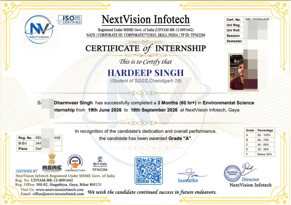
Internship Certificate
Tap to view
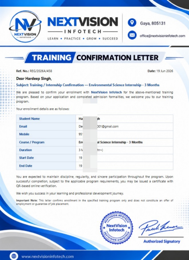
Joining Letter
Tap to view
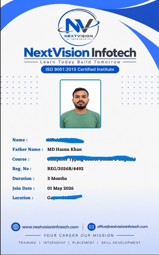
Student ID Card
Tap to view
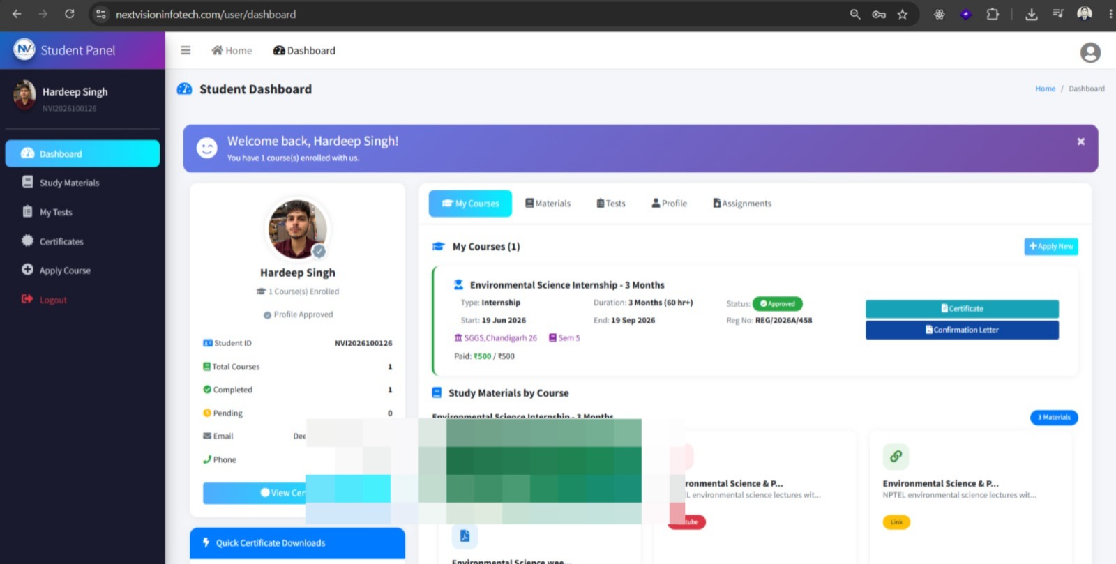
Student Panel
Tap to view
All certificates are issued by NextVision Infotech & are verifiable upon request.
Ready to Start Your Journey?
Take the first step towards your dream career with our internship programs